![]()
![]()
![]()
![]()
![]()
![]()
RF2TTC INTERFACE MODULE
Last updated: 18/03/2011 15:35

18/03/2011: latest release of the RF2TTC manual (5.3)
14/07/2009: release of the RF2TTC manual (5.2)
24/06/2009: New release of the RF2TTC manual (V5.1), matching the latest firmware version (25062009) - orbit length modifications
24/06/2009: New release of the RF2TTC manual (V5.0), matching the latest firmware version (24062009) and explaining how to calibrate the orbit fine delay
24/09/2008: New doc available: Transient states of RF2TTC output clocks
30/07/2008: all the modules are available and have been distributed (2 per experiment)
16/05/07: the 18 last modules are being produced and are expected for mid-june
01/05/07: the 2 pre-production modules have been validated. One is currently used by the experiments, the other one is used as a reference by PH/ESS
30/01/07: One prototype, together with Digital Tx and Rx modules, are evaluated by experiment.
11/12/06: The RF2TTC has been mostly tested. The results can be found in the system test report
11/12/06: The document gathering the VME mapping & the user manual of the board is available
11/12/06: A second prototype is being assembled and will be available for experiments beginning of January
DOCUMENTS:
RF2TTC user manual revision 5.1 - submitted 25/06/09
RF2TTC User Manual revision 5.0 - submitted 24/06/09
Review: TTC project page on the Indico Server
RF2TTC User Manual revision 2.0 - last submission: 16/05/2007
A production test procedure has been prepared, together with a C library to simplify the test as much as possible. This is a part of the RF2TTCscope software, available on the CVS repository.
RF2TTC test results
Schematics and Layout of the RF2TTC: EDA-01357
CVS repository for RF2TTC control software
Analysis of the board layout with SpecctraQuest, made by Alexandra Dana Oltean Karlsson, to understand the differences between the BCref and the other Clock paths (40ps rms jitter instead of 26): board analysis, vias extraction
VHDL code of the FPGA.
Money spent of the RF2TTC on 12/12/2006: Prototype paid by PH/ESS, production by the experiments.
updated price of the RF2TTC (1 board, Study deduced): 2500 CHF
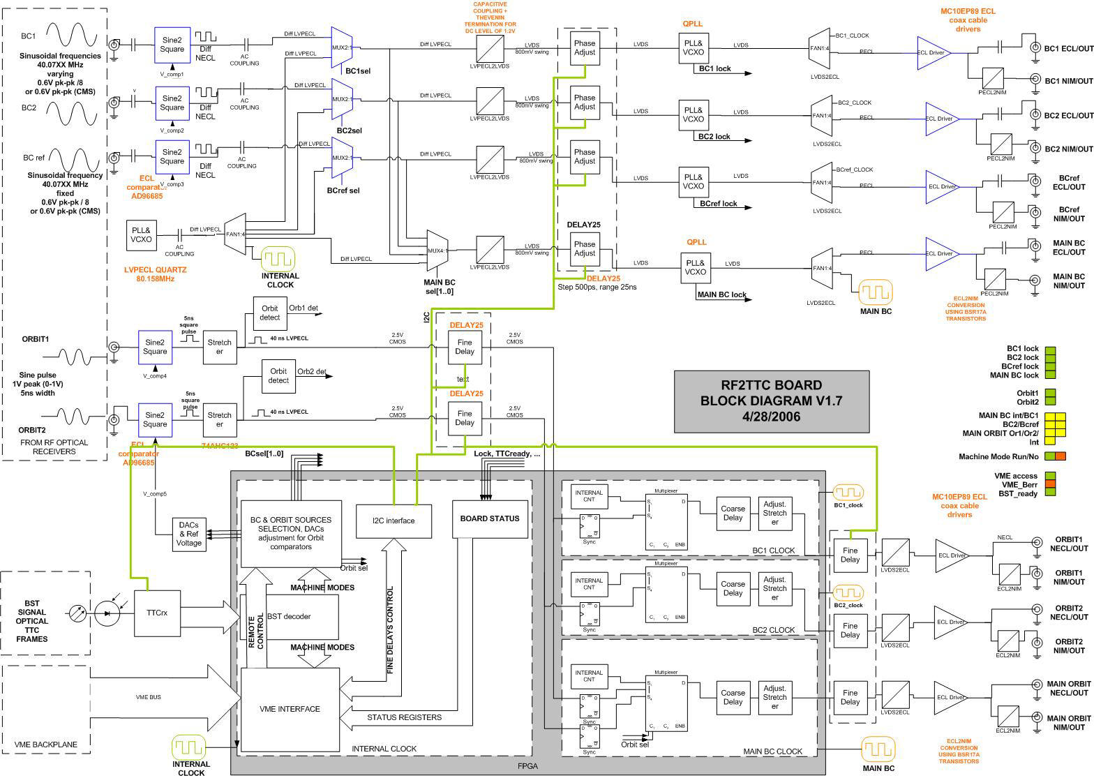
The RF2TTC module will act as an interface between the AB/RF optical receiver modules and the TTC system within the experiments. It will replace the TTCmi and bring some new functionalities like remote monitoring and control...
The RF2TTC is converting the three 40.078MHz Bunch Clocks (BC) and the two orbit signals from the RF optical receivers to ECL signals, and proposes various adjustments on each signal before making them available for the in-detector TTC electronics.
Form Factor:
The board is a 6U-4TE VME64x module.
Power supplies:
The standard voltages available on the power supplies of the TTC crates are +5V, +/-12V, +3.3V and 48V. The ALICE CTP crates, however, have no 48V.
To keep the compatibility between all the users, the RF2TTC will thus only use the following voltages:
As the VME specification allows only 1.5A per pin, the maximum current per board will be 9A for the 5V and the +3V3, and 1.5A per +/-12V each).
Technologies:
![]()
Inputs and Outputs:
Inputs:
Two types of inputs are available on the RF2TTC Front Panel:
The RF timing inputs are directly taken from the RF Rx modules. As 3 BC types and 2 Orbit types can be delivered by these modules, 5 inputs are foreseen in the front panel. To simplify, ‘Orbit’ is used for Frev or Orbit indistinctively.
Outputs:
It is proposed to provide 1 pair of ECL and NIM outputs per input, plus one pair of MAIN BC (ECL and NIM) and MAIN ORBIT (ECL and NIM). The connectors used for the outputs are Lemos.
Bunch Clocks:
The direct pairs of BC outputs are just simply the converted inputs, cleaned by a QPLL. It is possible to switch remotely the BC sources from inputs to the internal clock to work in stand-alone mode. The phase of each BC signal can be independently adjusted.
The MAIN BC is multiplexed between BC1, BC2, BCref and the internal clock.
Each ECL output is AC-coupled.
Orbit:
The direct pairs of Orbit are synchronized to their relative Bunch Clocks (BC1 for the Orbit of ring1 and BC2 for the Orbit of ring2) and stretched with an adjustable length. To ensure a stable synchronization, the input orbit phases are also adjustable, as well as the orbit outputs. It is as well possible to switch the Orbit sources from input to internal counters.
The MAIN ORBIT is synchronized to the MAIN BC, and multiplexed between Orb1, Orb2 and an adjustable internal counter running at the MAIN BC frequency.
Each ECL output is NECL-DC coupled.
Control Functions:
VME registers:
The CSR space (AM 0x2F) will contain the board ID as well as the BAR (Board Address Register).
The other access types will be reduced to D32/A32 (AM 0x09). To simplify the firmware, the board will not answer to D8 and D16 requests.
The mapping is cut in various blocks, one per each output, plus the BST interface and some general purpose registers. The blocks do not have consecutive addresses. Each block has a simple offset to ease the access and to allow some reserved space.
The interrupt lines are wired and thus available. Nevertheless, as CMS and LHCb may want to use VME masters handling interrupts, they should not be necessary in normal modes. They may be implemented as flags.
The Board address (8 bits) is manually configurable using rotary switches. The address 0 is not considered as a manual address, but indicates that the Board address is set by the geographical addressing facility.
Block Diagram (FINAL 02/05/06):
![]()
Last Updated by Sophie BARON on 18/03/2011 15:35